
Alright, buckle up buttercups, because we're diving headfirst into the glamorous world of… printed circuit boards! Yes, you heard right. Prepare to be mildly entertained, possibly even enlightened, as we unravel the mysteries of these green, often confusing, marvels of modern technology. Think of it as extreme dot-to-dot for engineers, only instead of a picture of a duck, you get… well, something that hopefully powers your toaster.
Component Placement: Where the Magic Happens (or Doesn't)
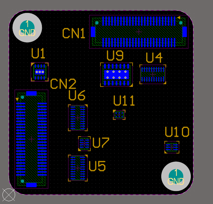
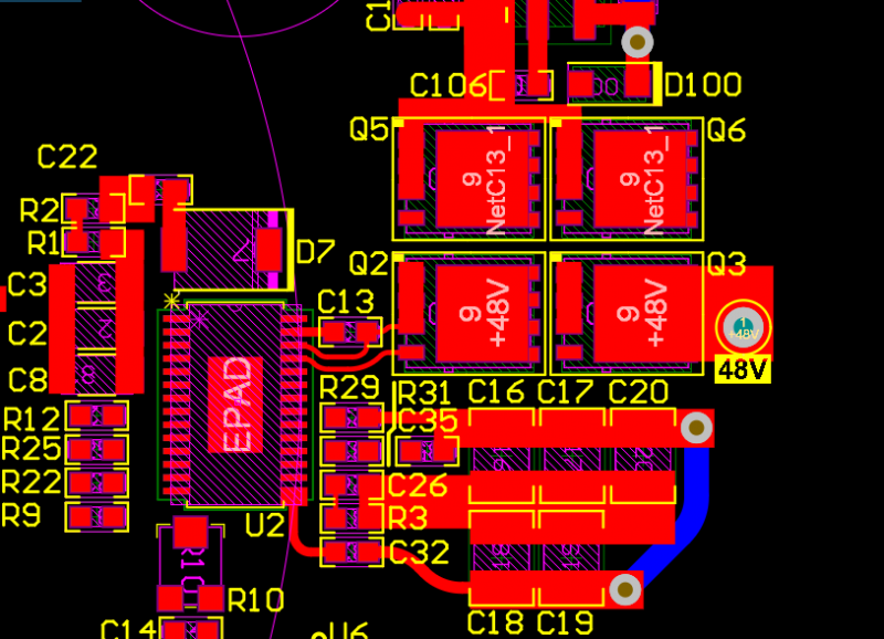
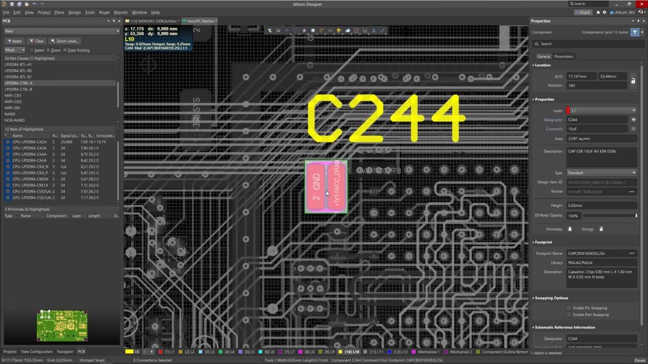
Behold! A visual representation of the sacred art of component placement. It's like playing Tetris, except if you screw up, your microwave might explode. Seriously though, placement is crucial. It's not just about shoving things wherever they fit; it's about optimizing signal flow, minimizing interference, and ensuring your board doesn't spontaneously combust. Notice the strategic arrangement of… stuff. Resistors, capacitors, those little black things that look like spiders… They all have a specific purpose, and if you put them in the wrong spot, things get… spicy. Imagine building a house and putting the plumbing in the attic. That’s kind of what bad component placement is like. Messy, expensive, and ultimately, a bad idea.
You see those little lines snaking around? Those are traces, the tiny highways for electrons. They’re like the veins and arteries of your electronic creation. You want them short, sweet, and direct. Think of them like your route to the coffee machine in the morning: the shorter, the better. Nobody wants a convoluted coffee journey, and electrons feel the same way. Too much resistance, and they get sluggish and grumpy. And grumpy electrons lead to grumpy circuits, which leads to grumpy engineers. It’s a vicious cycle, really. Now, someone needs to invent a PCB design software that also makes coffee. That would truly be revolutionary.
Castellated Circuit Boards: A Design So Clever, It's Almost Suspicious
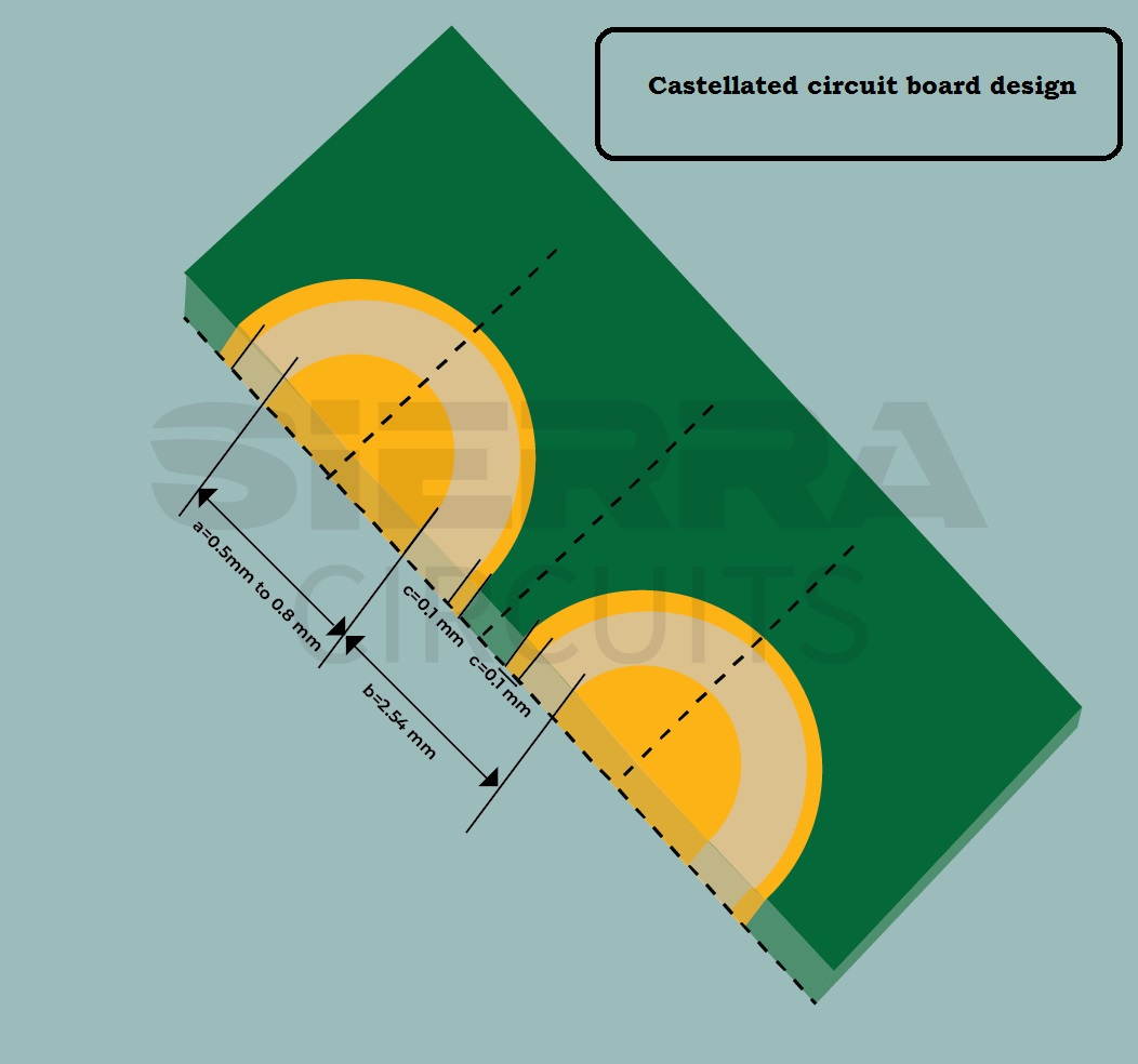
Feast your eyes upon the majestic castellated circuit board! Or, as I like to call it, the zig-zaggy wonder. See those half-moon shapes along the edge? Those are castellated holes, and they're not just for show. They're a clever way to connect multiple boards together, kind of like Lego bricks for electronics. But way more precise, and significantly less likely to end up embedded in your foot. They allow you to solder one board directly onto another, creating a seamless (or at least, a cleverly disguised seam) connection. Think of it as electronic origami. Functional, elegant, and possibly mind-bending.
Why go to all this trouble, you ask? Well, imagine you're building a tiny, super-efficient widget, and you need to cram as much functionality as possible into a small space. Castellated PCBs allow you to stack boards on top of each other, saving precious real estate. It's like building up instead of out. Plus, they offer excellent electrical conductivity, ensuring a clean and reliable connection. They're particularly useful for modules that need to be easily attached and detached. So, the next time you see a castellated edge, remember that it represents ingenuity and a healthy dose of engineering wizardry. And maybe a little bit of caffeine. Because let's be honest, nobody designs PCBs without copious amounts of caffeine.
And there you have it! A whirlwind tour of the wonderful world of PCBs. Now, go forth and create something amazing... or at least something that doesn't short-circuit the first time you plug it in.
If you are searching about Altium Designer vs. Eagle Software: Pros and Cons | Altium.com you've came to the right web. We have 25 Pictures about Altium Designer vs. Eagle Software: Pros and Cons | Altium.com like Simple Placement | Altium Designer 25 and 24 Technical Documentation, Simple Placement | Altium Designer 25 and 24 Technical Documentation and also Streamline Your Product Development - Altium 365 Cloud PLM Integration. Read more:
Altium Designer Vs. Eagle Software: Pros And Cons | Altium.com
 www.altium.com
 altium designer cons eagle pros software vs routing
Making Projects Available Online | Working With Altium 365 | Video
 my.altium.com
 PCB Schematic Design: In 10 Schritten Zur Leiterplatte | Altium
 resources.altium.com
 altium pcb schaltplan lm358 amp amplifier einfachen pcbs erstellt module vollständigen tausend erstellen schematics automatisch progettazione finished schémas schaltkreis leiterplatte
Streamline, Collaborate, And Innovate With PLM In PCB | Altium
 resources.altium.com
 Tutorial Altium Designer 18 Membuat Pcb Dengan Altium Designer 18 | Hot
 www.hotzxgirl.com
 Getting Your Layer Stack Right | Whitepaper | Altium
 resources.altium.com
 altium pcb arduino circuit impedance stack mentor pads stackup calculator trace versus multilayer circuits driven constraints editing mcad placing planes
Altium Designer Printed Circuit Board PCB Computer Software, PNG
 favpng.com
 Pcb Design Process Flow At Louise Whipple Blog
 storage.googleapis.com
 Pcb Design Using Altium
 studyzonefiranemometer.z13.web.core.windows.net
 Advantages Of Using Draftsman To Create A PCB Assembly Drawing | Design
 resources.altium.com
 Altium Designer Pcb Extension - Sexisecure
 sexisecure.weebly.com
 Altium Designer 24 现已发布| Altium
 www.altium.com.cn
 Altium Designer Webinar: Altium Designer 24 - Thiết Lập Tiêu Chuẩn Mới
 cae-solutions.vn
 Simple Placement | Altium Designer 25 And 24 Technical Documentation
 www.altium.com
 Altium Designer Pricing, Cost & Reviews - Capterra UK 2025
 www.capterra.co.uk
 Simple Placement | Altium Designer 25 And 24 Technical Documentation
 www.altium.com
 Altium Multi-Board Schematic: Streamline Your Design Process – Hillman
 hillmancurtis.com
 Streamline Your Product Development - Altium 365 Cloud PLM Integration
 resources.altium365.com
 Altium Designer Pcb Layout
 schematiclistwandered.z14.web.core.windows.net
 Streamline Your Product Development - Altium 365 With Arena
 go.altium.com
 How To Design A Castellated Circuit Board | Sierra Circuits
www.protoexpress.com Altium Designer - PCB Design Software
 www.altium.com
 altium designer pcb design software interface experience modern
Component Placement | Create Your Own PCB | Video Tutorials | Learn
my.altium.com placement component pcb layer altium
Streamline Document Creation And Management | Altium
 resources.altium.com
 streamline pdf creation document management altium
PCB Process Flow Chart | Www.homillux.com
 www.homillux.com
 Altium designer pcb design software interface experience modern. Streamline document creation and management. Pcb design using altium